We often work with design engineers, managers and business owners who are not sure how to make their applications comply with electromagnetic compatibility (EMC) regulations. Here are six best practice tips for minimizing electromagnetic interference (EMI) issues in electronic systems.
Component Placement
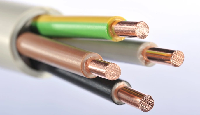
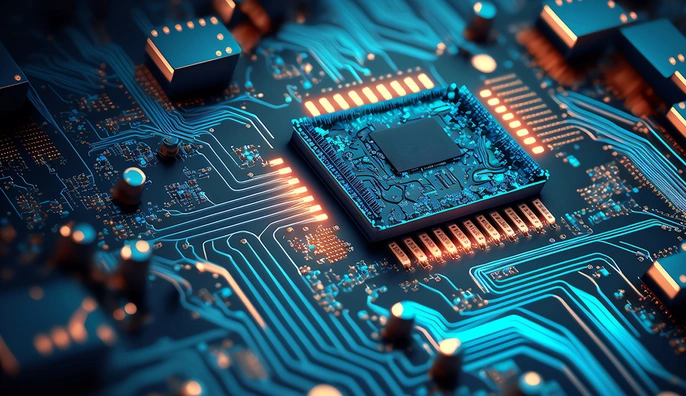
Where components are placed on a printed circuit board (PCB) or in any kind of product can have a significant impact on the degree that signal coupling is minimized and how much EMI is reduced. Components need to be arranged to minimize trace lengths and it is important to keep high-speed signal paths away from sensitive components. Also, avoid the creation of loops that could act as antennas. Make sure that EMI filters are always placed close to the source, that distances are kept as short as possible everywhere on the circuit board or free wiring, and that there is a good impedance to ground so that disturbances can be fed back.

Power Distribution
Power distribution networks should be designed to keep voltage drops, noise and ripple as low as possible. If decoupling capacitors are strategically placed near power pins of integrated circuits, this can help to filter out high-frequency noise and provide stable power delivery. If distribution of power is limited to certain areas, this will prevent it from spreading out over the rest of the circuit.


Signal Integrity
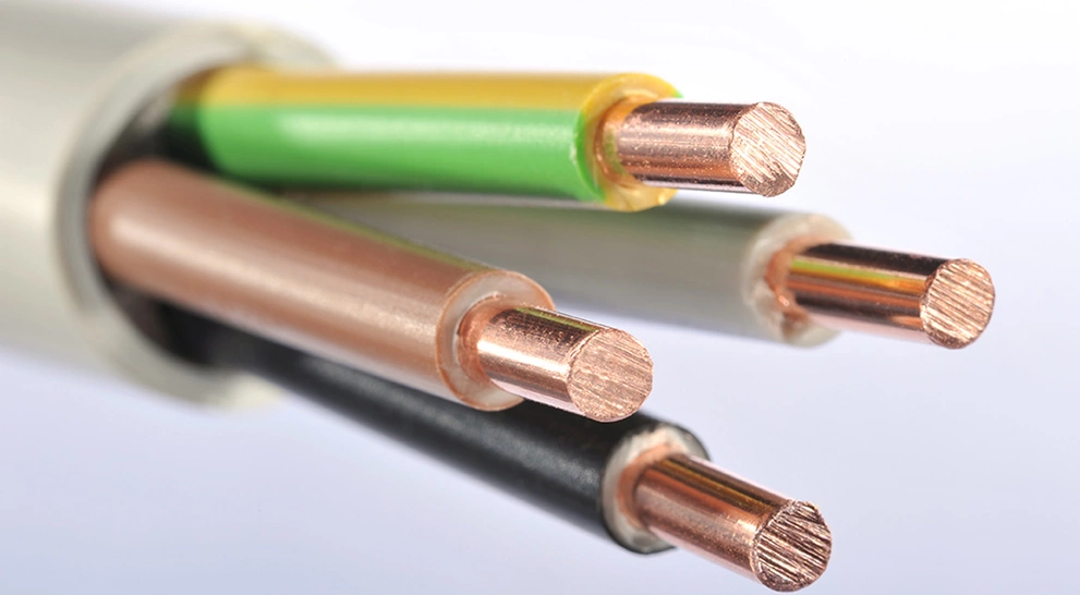
Maintaining signal integrity is essential and can be achieved by controlling impedance, minimizing signal reflections and using proper termination techniques for high-speed signals. Matching trace lengths for differential signals will help to prevent skewing and ensure reliable data transmission. Always remember that the two input and output cables must never run alongside each other, they should always be crossed in orthogonal way. Of course, this is the case for all electronic applications, not just PCBs.
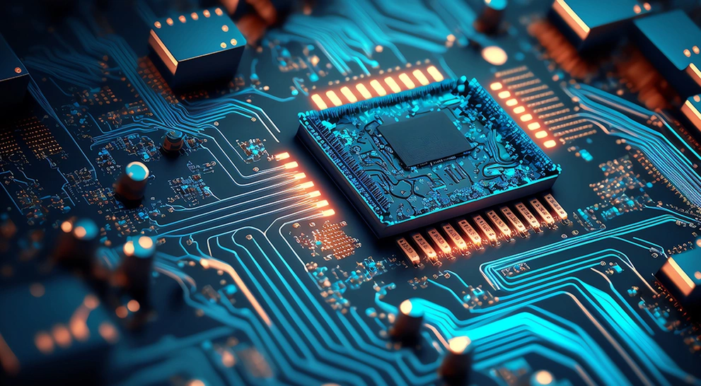
Routing
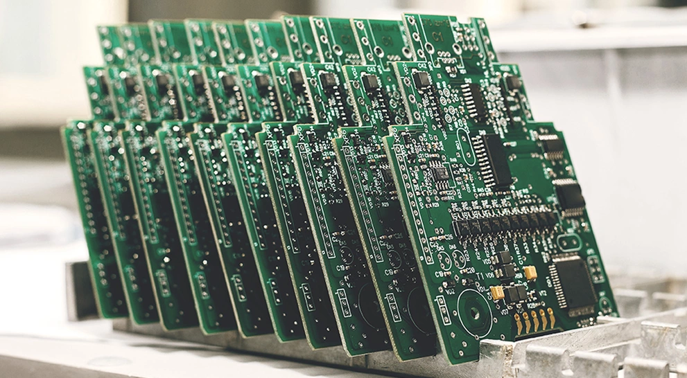
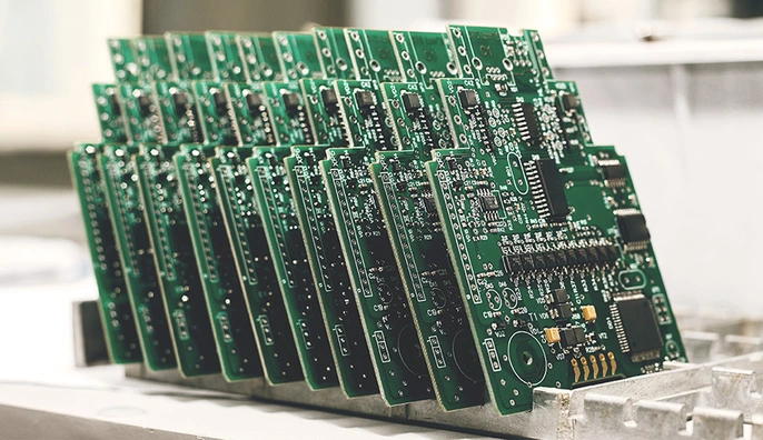
This comes under the areas of power distribution and signal integrity and requires design engineers to follow best practices when routing high-speed signals, including differential pairs, clock signals and high-frequency traces. Not only do designers need to look at minimizing trace lengths, but they should also avoid sharp bends and maintain consistent trace widths to minimize signal degradation and EMI.
Stack-Up Design
This also relates to power distribution and requires engineers to optimize PCB stack-up to keep down crosstalk, impedance mismatches and EMI. Factors they need to consider include layer count, signal layer placement and using dielectric materials to achieve optimal levels of signal integrity and EMC performance.
Ground Isolation
This is important because isolating sensitive analogue or digital circuitry on separate ground regions can prevent coupling of noise between different circuit blocks. Star grounding or partitioning techniques are ideal for segregating noisy and sensitive circuitry.
By following these best practice tips, design engineers will go a long way towards mitigating most EMC issues.